1 Nov 2026
Tracing Fabrication Hurdles in Crafting Precise Microscopic Spires
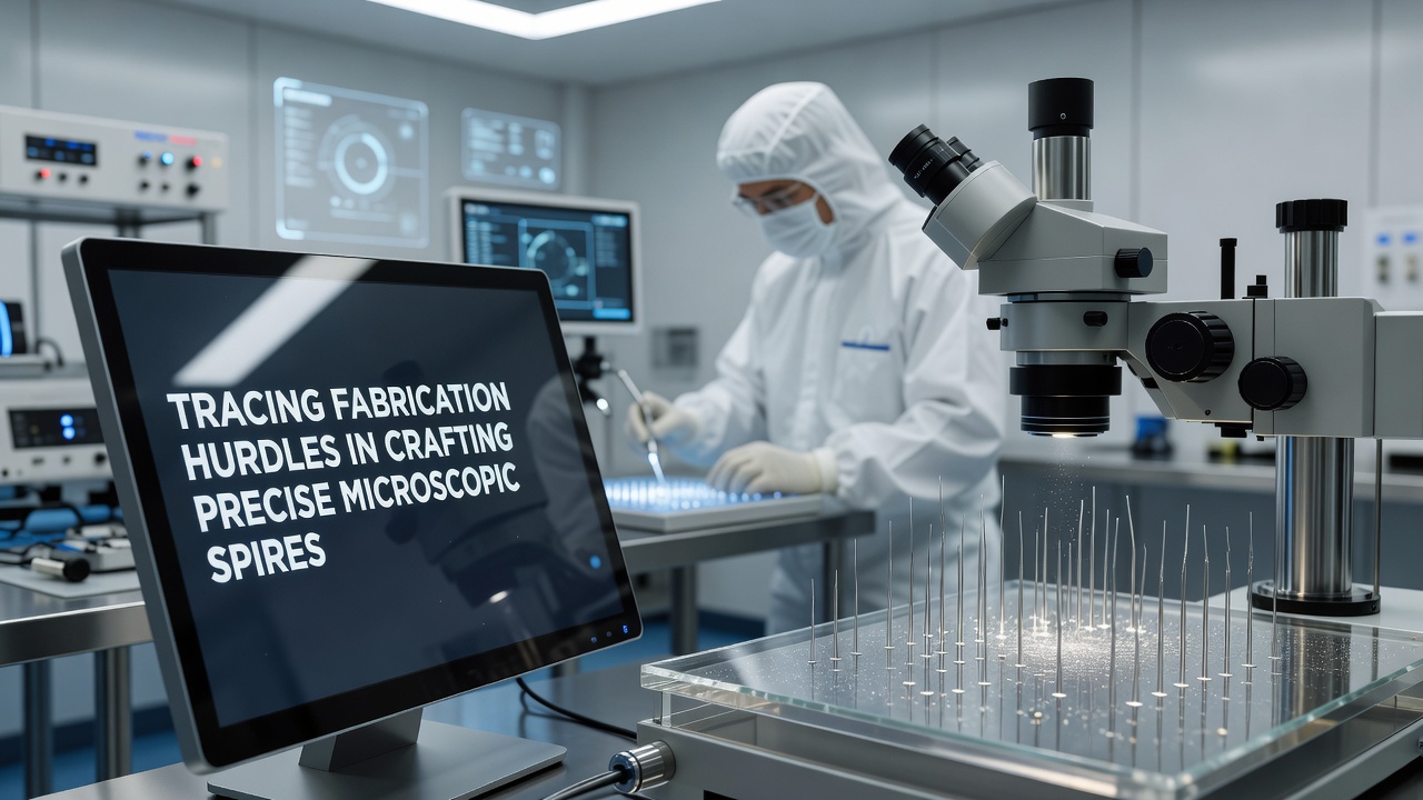
Engineers and materials scientists continue to encounter significant obstacles when attempting to produce microscopic spires with consistent precision at the nanoscale, and these hurdles stem from fundamental limitations in current deposition and etching processes. Data from multiple research facilities indicate that achieving uniform height and tip sharpness across arrays requires control over variables that often interact in unpredictable ways during production runs.
Material Deposition Challenges
Deposition techniques such as chemical vapor deposition and atomic layer deposition must operate within narrow temperature and pressure windows to avoid defects, yet even minor fluctuations can lead to uneven layering that compromises the final spire geometry. Researchers at institutions across North America and Europe have documented how precursor gas flow rates influence sidewall smoothness, with studies showing that deviations as small as 0.5 percent can introduce surface roughness exceeding acceptable tolerances for applications requiring sub-10-nanometer accuracy.
Thermal expansion mismatches between the substrate and deposited materials create additional stress points during cooling phases, and these stresses frequently result in micro-cracks that propagate under subsequent processing steps. Observers note that monitoring systems installed in cleanrooms have captured real-time data revealing how rapid temperature ramps exacerbate these issues, prompting many facilities to adopt slower, multi-stage heating protocols that extend overall fabrication times.
Etching and Pattern Transfer Limitations
Plasma etching processes used to define spire shapes face constraints related to anisotropy and selectivity, where the etch rate must remain uniform while stopping precisely at designated depths. Figures from equipment manufacturers reveal that ion bombardment angles shift slightly across larger wafers, leading to variations in spire base widths that accumulate across a single batch. Focused ion beam milling offers higher precision for small-scale prototypes, but scaling this method to production volumes encounters throughput bottlenecks because each structure requires individual rastering.
Alignment errors during multi-layer lithography steps compound these difficulties, particularly when overlay tolerances drop below 2 nanometers. Industry reports from 2025 highlight cases where mask distortions caused by electron beam exposure created cumulative offsets that rendered entire arrays unusable, and corrective algorithms developed since then have reduced but not eliminated such misalignments.
Contamination and Environmental Controls
Particle contamination remains a persistent problem in high-vacuum chambers, where even trace amounts of residual gases can deposit onto growing structures and alter their electrical or mechanical properties. Monitoring data collected through November 2026 at several advanced fabrication centers shows seasonal variations in ambient humidity affecting filter performance, which in turn influences defect densities observed in finished spires.
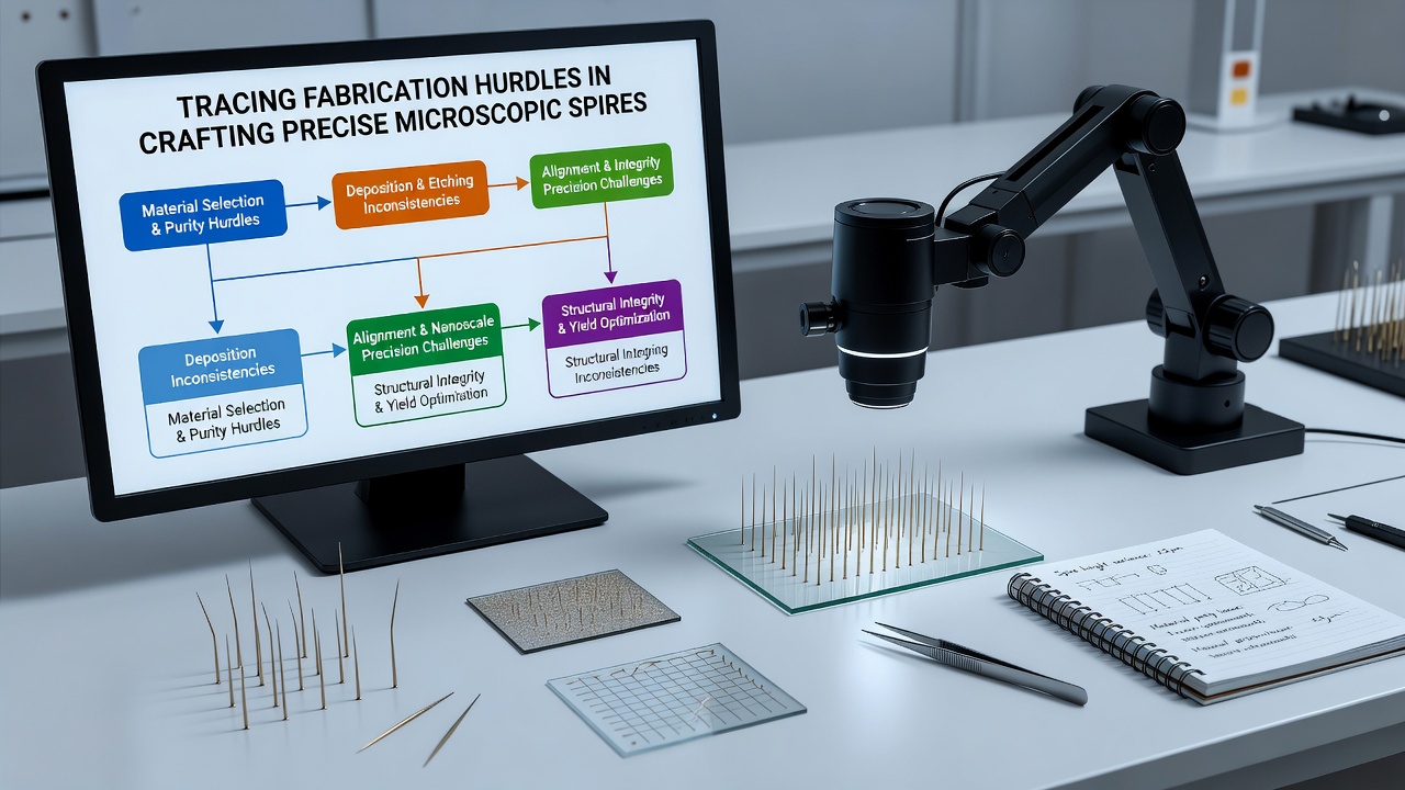
Researchers have traced some yield losses to electrostatic discharge events that occur during handling between process tools, and these events become more frequent as feature sizes shrink because charge accumulation increases relative to the structure volume. Mitigation strategies involving conductive coatings and grounded fixtures have shown measurable improvements in controlled tests, according to findings published by collaborative groups spanning Australian and Canadian laboratories.
Measurement and Verification Difficulties
Verifying the exact dimensions of completed microscopic spires presents its own set of hurdles, since conventional optical metrology lacks the resolution needed at these scales. Scanning electron microscopy and atomic force microscopy provide detailed surface maps, yet sample preparation for these instruments can introduce artifacts that obscure true fabrication outcomes. Data compiled by international standards bodies indicate that inter-laboratory comparisons often reveal discrepancies of several nanometers in reported heights, underscoring the need for standardized calibration protocols.
One study revealed that tip convolution effects in atomic force measurements systematically overestimate spire apex radii, leading teams to develop deconvolution software that adjusts raw datasets before analysis proceeds. Such computational corrections have become standard practice in many facilities, though their accuracy depends on precise knowledge of probe geometry which itself varies over time.
Emerging Approaches and Ongoing Research
Recent advances in machine learning-assisted process control have allowed operators to predict and compensate for some deposition variations in real time, and preliminary results from pilot lines suggest these systems can improve batch consistency by measurable margins. Yet the underlying physics of material interactions at the nanoscale continue to impose boundaries that software alone cannot overcome.
Collaborations between academic groups and equipment suppliers have produced new precursor chemistries designed to reduce stress during deposition, with testing phases scheduled through late 2026. These efforts build on earlier work documented in peer-reviewed journals, where researchers demonstrated that incorporating stress-relief interlayers could extend the viable aspect ratios for spire structures without inducing cracks.
Conclusion
Tracing fabrication hurdles in crafting precise microscopic spires reveals a landscape shaped by interconnected physical constraints, metrology limitations, and environmental sensitivities that demand coordinated advances across multiple disciplines. Continued collection of process data alongside refinements in tooling and materials offers pathways toward higher yields, while international cooperation among research entities helps standardize approaches that address the most persistent challenges.